I often get asked to look at such-and-such Wikipedia entry, or someone is trying to convince me of something and using a Wikipedia entry as a "reference" to back up his/her argument. It is usually during such instances that I find inaccuracies, confusing statements, and something outright errors in such entries. I was doing my own search on something a few minutes ago, and I decided, out of curiosity, to see what Wikipedia has to say about "Work Function". Now, keep in mind that this is a common terminology, especially for physics students, since the photoelectric effect is a "must-know" topic for these students. One would think that this should be a topic that a Wikipedia entry would get it right, considering how many people would look up such a thing, AND, the fact that errors and inaccuracy would, by now, be ironed out.
WRONG!
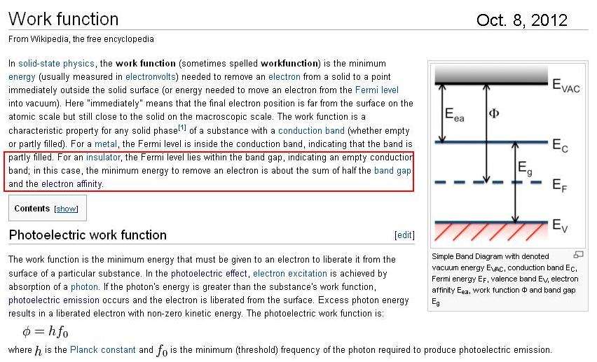
This is what I saw on the Wikipedia page TODAY.
I posted today's date in the screen capture as a date stamp on when this was viewed.
The offending passage has been highlighted with a red box. Let's look at it closely, shall we?
The description here is on what happened for an insulator (or a semiconductor, for that matter). The figure shown is the simplified band diagram for such a system (i.e. an intrinsic semiconductor, for example), and defines the various quantities such as the work function, band gap, electron affinity, etc. The problematic statement says this:
For an insulator, the Fermi level lies within the band gap, indicating an empty conduction band; in this case, the minimum energy to remove an electron is about the sum of half the band gap and the electron affinity.The first part of that paragraph which says ".... For an insulator, the Fermi level lies within the band gap, indicating an empty conduction band ..." is OK. However, the second part is very puzzling and an outright error : "... in this case, the minimum energy to remove an electron is about the sum of half the band gap and the electron affinity ..."
Whoever wrote this is STILL thinking that the work function (Phi) is still the minimum energy needed to produce photoemission, as in the case of a metal. This is FALSE, and anyone who looks at the band diagram can tell. Half of the band gap plus the electron affinity is the work function Phi, but this is the energy between the vacuum level and the Fermi level. The Fermi level for insulator/semiconductor has NO STATES, and thus, no electrons to excite! After all, it resides in the band gap! So what is being excited here?
For an insulator/semiconductor, while the work function may still be defined as the energy between the Fermi level and the vacuum level, it no longer corresponds to the photoemission threshold! The photoemission threshold now is the full band gap energy PLUS the electron affinity. You need to excite, at the minimum, the electrons from the top of the valence band to the vacuum level. One can see this clearly by looking at the band diagram in the figure.
I hope no one was using on this Wikipedia entry for something useful or important.
Zz.

6 comments:
Did you fix it? Why hate on wiki without editing it? Be the change you want to see in the world.
You need to learn how to read AND comprehend. I could spend a lifetime correcting it, and it will still not change my opinion of it. It is FUNDAMENTALLY FLAWED!
Zz.
Hum. Been a while since I refreshed my memory on band gaps and such stuff. If I followed you correctly, isn't the first sentence of the Wikipedia entry also false?
"the work function is the minimum energy needed to remove an electron from a solid ..."
Shouldn't it be "the work function is defined as the energy difference between the vacuum energy level and the Fermi level of a solid"? I've just rooted out a solid materials book from our lab library and it refers to the energy needed to extract an electron from a semiconductor via a photon as the "photothreshold" = Evac - Ev
But I suppose all that is irrelevant as it doesn't address the fundamental flaw of Wikipedia. Of course, it begs the question of why doesn't anybody start up a peer-reviewed equivalent of Wikipedia? Not as competition per say, but as a compliment. I suppose time and money are the main barriers to such a project?
Cheers.
"Hum. Been a while since I refreshed my memory on band gaps and such stuff. If I followed you correctly, isn't the first sentence of the Wikipedia entry also false?
"the work function is the minimum energy needed to remove an electron from a solid ..."
Shouldn't it be "the work function is defined as the energy difference between the vacuum energy level and the Fermi level of a solid"? I've just rooted out a solid materials book from our lab library and it refers to the energy needed to extract an electron from a semiconductor via a photon as the "photothreshold" = Evac - Ev"
If you look at the band diagram, you'll notice that "Evac - Ev" IS equal to the electron affinity plus the band gap!
I don't see a problem with that definition of the work function - FOR A METAL. This is because, as I've said, the work function, the electron affinity and the location of the Fermi level are all the same in a metal. In a semiconductor, they are not.
Zz.
For what it's worth, I've added a discussion to the talk page of the Wikipedia "Work Function" article:
https://en.wikipedia.org/wiki/Talk:Work_function
Thanks Garrett.
Post a Comment